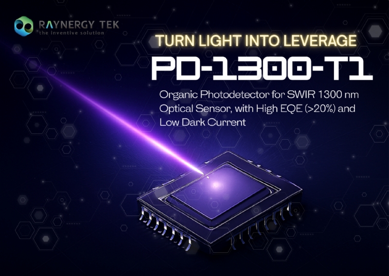
Isorg and Raynergy Tek Join Forces to Develop Organic Photodetectors for Consumer Electronics Market

This collaboration marks an important step towards advancing OPD SWIR technology to launch next generation products

Isorg, a pioneer in Organic PhotoDetectors (OPDs) and large area image sensors, and Raynergy Tek, a leader in organic semiconductor announce the signature of a Joint Development Agreement to accelerate the development of OPD technology for short-wave infrared (SWIR) image sensors and detectors, which can be applied on next-generation biometric authentication on consumer electronics products.

According to Yole Group, an expert in the analysis of technology markets, the SWIR image sensor value market is expected to reach $2.9 billion by 2028, as SWIR imaging provides more detailed information than visible and near-infrared lighting. The existing silicon-based CMOS image sensors have no spectral response to SWIR light, and alternative inorganic semiconductors, such as InGaAs are too expensive to be integrated into consumer electronics products.

On the contrary, organic semiconductors can achieve SWIR light response by designing the molecular structure of polymers; this allows to create a photodetection layer using non-toxic and heavy-metal free materials with low-temperature, non-vacuum and fast processes, which bring more benefits than competing technologies.

This partnership is a major step forward for the development of OPD SWIR technology. Isorg has a strong technical background in OPD processes on different types of substrate including CMOS wafer, as well as device manufacturing, while Raynergy Tek is an expert in organic semiconductor materials: The combined focus of both companies will ensure the success of OPD technology in high volume applications in consumer electronics.

“We have been very active to develop evaluation platforms and application prototypes to address smartphones, VR headsets, healthcare and biometry applications. The collaboration with Raynergy Tek is an important activity to achieve the successful integration of SWIR based on OPD technology for next generation products” said Dieter May, CEO of Isorg.

Phoebe Tan, CEO of Raynergy Tek emphasized “we recently had a breakthrough in R&D, our proprietary materials showed remarkable SWIR response, the detectivity is up to 1011 Jones at 1300nm wavelength. The collaboration with Isorg is very important to demonstrate readiness and viability of our material for commercial development at fab level.”

About Isorg
Isorg is a pioneer in organic and printed electronics for large area photodetectors and image sensors. It offers a new generation of high-performance imagers with the capability for easy integration into systems with various shapes or form factors. Its flexible image sensors have application in consumer electronics, ID security and access control, IoT and medical devices. In 2020, it launched the first worldwide demonstrator of full-screen sized Fingerprint on Display (FoD) for smartphones. A year later, it received the first worldwide FBI certificate for an organic photodiode-based fingerprint module for the security & ID market. Founded in 2010 and partnering with CEA-Liten, a leading French innovation center for new energy technologies and nanomaterials, Isorg has attracted substantial investments.
www.isorg.fr

Isorg Media contact
contact.media@isorg.fr

About Raynergy Tek
Raynergy Tek, the leader in innovation, research and development, manufacturing and commercialization of Organic-based Semiconductors (OSCs) materials. Their proprietary material is used for cutting edge optoelectronics devices on image sensing electronics products and energy harvesting solar cells.
www.raynergytek.com

Raynergy Tek Media contact
info@raynergytek.com

We are pleased to announce that Raynergy Tek is certified ISO 14001:2015 by DNV

Taking care of our environment, and preventing our company from causing negative impacts on the environment, are two of the most important challenges facing businesses today. One of the biggest intention of implementing an Environmental management system to show our commitment are among those businesses that care enough to reduce our environmental footprint. We care for our environment and wanted to ensure we use all the resources in the best way we could.

Consistent with the Raynergy Tek’s environmental policy, we are pleased to announce that, today we have received and achieved our second ISO certification target this year i.e. ISO 14001:2015 by DNV.

Kudos to our ISO special action team led under Howard, Katy, Benny, Mingchen and Yachun, they worked diligently in the past 1 year to coordinate with all the key members in the company to implement the best practices that we could do and make sure we comply to all the obligations and standards to achieve this certification!

Epishine and Raynergy Tek Forge a Stronger Partnership to Drive Innovation in Sustainable Indoor Solar Cells

Market-leading indoor solar cell manufacturer Epishine and advanced organic semiconductor supplier Raynergy Tek announce the signing of a supplier agreement. This strategic partnership represents a milestone in their shared commitment to advancing the field of indoor solar cell technology through collaborative efforts and combined expertise in their respective fields.

With the rapid growth of IoT devices, the European Commission predicts that a staggering 78 million batteries will be discarded daily by 2025. The urgent need for a sustainable solution to address this issue has never been more critical.

Epishine has established itself as a market leader in indoor solar cells, providing high and reliable performance in low light conditions. Epishine is firmly dedicated to maintaining exceptional quality and manufacturing excellence through their patented production process. Given that an application powered by indoor solar cells must be adapted to the lowest measured output of the module, Epishine emphasizes the importance of consistent performance over occasional high peaks in performance.

Jonas Bergqvist, CTO at Epishine, emphasizes, “Our commitment to quality is a key factor in establishing reliable partnerships with industry leaders like Raynergy Tek. We are extremely optimistic about this partnership and the potential benefits for both parties.”

This partnership marks an important step towards ensuring reliable material supply as Epishine scales up its production to meet the demand for billions of units. Additionally, an in-depth material quality inspection system has been established, which includes characterization of materials under typical indoor conditions. Manufacturing excellence and access to the most innovative materials on the market are both imperative for the further development of Epishine’s market leading indoor solar cells.

Benny Lin, Vice President at Raynergy Tek, highlighted that, “The integration of OPV technology in IoT devices is highly anticipated to commercialize and we are confident that Epishine will be the leader in this space. As our commitment to excellence, we are thrilled to share that we’ve recently achieved ISO 9001:2015 certificate to deliver quality management and quality assurance to partners like Epishine.”

About Epishine: Epishine is a leading developer and manufacturer of printed organic solar cells, committed to reducing global environmental impact by enabling innovative and smart technologies to meet the growing demand for sustainable energy solutions. Epishine's business is based on pioneering manufacturing breakthroughs. Their flagship product is a unique indoor solar cell optimized for harvesting indoor light and easily integrating into small low-power electronics.

About Raynergy Tek: Raynergy Tek is the leader in innovation, research and development, manufacturing and commercialization of Organic-based Semiconductors (OSCs) materials. Their material is used for cutting edge optoelectronics devices on energy harvesting solar cells and light/image sensing electronics products.

PRESS CONTACT EPISHINE
Kristina Hagstedt
Communication Manager
kristina.hagstedt@epishine.com
+46 (0)73 466 63 43

PRESS CONTACT RAYNERGY TEK
Benny Lin
Vice President of Business Development
benny.lin@raynergytek.com
+886 (0)3 666 3266

We are delighted to share that a bio-signal sensor with organic photodetector from Raynergy Tek was successfully demonstrated.

Under a national program collaborated with Prof. Fang-Chung Chen from National Yang Ming Chiao Tung University, by using our proprietary organic semiconductor functional ink, PD-940, which is capable to sensor near infrared light up to 1000 nm, an oximeter-like device was made to detect heart rate and blood oxygen.

The needs of mobile bio-signal sensor are getting stronger these days for real-time health monitor, in order to get more bio-signals, such as blood glucose, a short-wave infrared (SWIR) light detector for mobile device is essential.

Raynergy Tek has been working on design a brand-new organic semiconductor material to sense SWIR light, we believe it is going to benefit human being for a healthy lifestyle in the future.

Happy to introduce our new Chairman, Ms. Joanne Hsiao!

Ms. Joanne Hsiao, a veteran in printing industry who has more than 20 years of experiences in Business development in Japan, Greater China, Europe and Taiwan, she is one of our founding and key shareholders from day one till today and have shown us unwavering supports throughout these years. Congratulations on the new role!

With new leadership in place, we will continue our laser focus in the acceleration of the development of the novel Organic photodetector proprietary materials for Eye Safety Sensor application.

Our outgoing Chairman, Jason will remain as one of the strong pillars of support in our Board of Directors as Supervisor who will constantly monitoring our development progresses. Thank you, Jason!

A new phase for Raynergy begins! Here we go!

Raynergy Tek is certified with ISO 9001:2015 by DNV!

A Quality Management System ensures we execute Plan. Do. Check. Act to quickly response, feedback, readjust, revamp to meet our quality assurance on product targets to our business partners. We pledge our systematic way of work planning, details recording with proper design on feedback loop that minimize wrongdoings and ensures we do not misfocus on the way to create win-win with our business partners.


From left to right Dr. Min-Hsien Chen, Dr. Chuang-Yi Liao and Prof. Ho-Hsiu Chou.

Raynergy Tek’s Organic Semiconductors (OSCs) could participate in hydrogen generation! Our OSCs served as photocatalysts for visible-light-driven boosting efficiency and stability!

Photocatalytic water splitting for hydrogen and oxygen generation are seeing a new wave of interests as it allows converting solar energy into chemical energy, and membrane-based operations could offer the possibility to achieve one-step hydrogen generation from water splitting at ambient temperature without needing further energy inputs, contributing to a so called “clean Hydrogen Economy”. Therefore, the pursuit of innovative photocatalysts which can enhance the photocatalytic activity is imperative and continuously gain increased interests in R&D of Hydrogen generation.

In collaboration with Prof. Ho-Hsiu Chou from National Tsing Hua University, Prof. Chou successfully developed a hydrogen energy technology that utilizes Raynergy Tek’s proprietary conjugated polymer dots (Pdots) as organic photocatalysts, enhancing the efficiency and stability of photocatalytic hydrogen evolution, which is an encouraging R&D results to advance the large-scale hydrogen production. We are particularly proud that this specific work has been published in Macromolecules, December 2022. Excitingly, this work was selected as the Front Cover of Macromolecules in February 28, 2023 (Volume 56, Issue 4).

To read more details on the research finding of how to use OSCs as the photocatalysts, please visit: https://pubs.acs.org/doi/10.1021/acs.macromol.2c02130

For further question, you may contact Prof. Chou hhchou@mx.nthu.edu.tw for more information.

ASCA and Raynergy Tek are strengthening their partnership

By using Raynergy Tek’s newest semiconductor materials, non-fullerene acceptor-based organic semiconductors and a new generation of hole transport layer, ASCA has achieved significantly higher OPV efficiency, beyond 70 watts per square meter while maintaining its durability. This is a 40 percent power increase compared to today’s industrial product.

In order to further improve and upscale with these materials, Raynergy Tek and ASCA are strengthening their long-lasting partnership through signing a Memorandum of Understanding.

On this occasion, an ASCA OPV structure, a concept of Zero-Energy Media Façade http://media-facade.asca.com/basel/ has been installed at Raynergy Tek’s new facility in Hsinchu Science Park, Taiwan.

We are very optimistic about the growth of OPV market and have common goal to bring theOPV business to next level.

To read more details, please visit: https://www.asca.com/news/asca-and-raynergy-tek-are-strengthening-their-partnership/

We are honored to provide in-kind support of organic semiconductor inks to the School of Electrical Engineering, NTU to use it for the undergraduates’ laboratory experiments that allows students to experience new technology that might impact the world tomorrow

This is a class that starts at 7 pm, a group of undergraduate students who are passionate about science, stay at the laboratory and eager to learn how science makes things happen!

Today, the management team of Raynergy Tek, Jason Hsiao, Yi-Ming Chang and Benny Lin returned to their alma mater, National Taiwan University (NTU). NTU is one of most prestigious tertiary education in Asia and one of the essential talent cultivation center to meet the continuous growth of semiconductor industry. Raynergy Tek is more than honor to provide in-kind support of organic semiconductor inks to the School of Electrical Engineering, NTU to use it for the undergraduates’ laboratory experiments. We are happy to involve in supporting the continuous innovation in education that allows students to experience new technology that might impact the world tomorrow.

Organic semiconductor technology for optoelectronics topics is on the rise these days thanks to the commercialization success of AMOLED in the display industry. What’s the next exciting application for Organic semiconductor is still on the quest! We believe that there are ample of possibilities with this technology. These years, it has earned a significant recognition for the forward making of green energy and futuristic sensors. We are glad that we have this opportunity to share the joy of making new science and technology happen to the new generation of students, who could be the next generation scientists and engineers to drive this technology forward.


R&D team leaders, from left to right Dr. Yi-Ming Chang (CTO), Dr. Kuen-Wei Tsai (R&D manager) and Dr. Chuang-Yi Liao (R&D director)

Raynergy Tek announces Novel Organic Semiconductors with spectral response of 1300 nm and detectivity of 1011 is within Reach !

We have achieved an important milestone in our Novel Organic semiconductor (OSCs) materials development. An OSCs material, PD-1300 which demonstrated good spectral response at wavelength of 1300 nm was developed by our R&D team successfully. The photodiode’s dark current density records an impressive value of 3x10⁻⁷ A/cm2 and detectivity tabulated to be 9.3 x 10¹⁰ Jones at voltage bias of -2 V, respectively, which to our knowledge is the best results of known reported for OPD-based SWIR device performance.

Generally, it is skeptical for organic semiconductor based photactive material to show spectral response of wavelength over 1000 nm, mainly attributed to the likelihood of recombinaton of the exciton generated by light within the ultra low bandgap material according to the known theoryof organic semiconductor. However, the prominent challenge was overcome by our materials designers and presents a strong candidate of materials for potential use in SWIR application. In addtional, the organic based photodiode device is made by solution, low temperature process and ink formulated using green solvent to be in line with low carbon emmision and ESG policy.

One of the key advantages of SWIR light is it can differentiate the objects which visible light cannot do, and offer better detectivity under objects due to higher transmmision. Therefore, the revolutionary SWIR image sensor is highly sought out and targeted to be widely adopted for under display 3D structuring for mobile phone authentication, eyes tracking for AR/VR headset, Lidar and camera for automotive ADAS or AD system etc. Besides, SWIR light is safer in operation for eye ball detection compared to that of NIR light, which make eye safety sensor a common future-sensor trend. As the latest market forecast from Yole Group, the SWIR image sensor might generate a value of $3.2B by 2027 with 52% CAGR since 2021.

This SWIR materials development project was started early this year, we are glad that the dedicated 10 months’ effort has significant results that could possibly propel us to next level materials innovation. We give the credit to our excellent R&D team led by Dr. Yi-Ming Chang (CTO), Dr. Chuang-Yi Liao (R&D director) and Dr. Kuen-Wei Tsai (R&D manager). We make science happen again! We will continue making it happen!


Figures:
(a) IV curve of PD-1300 device under bias from 2 to -2 V
(b) Detectivity of PD-1300 device shows spectral response ranges from 300nm to 1500nm

We are proud to demonstrate a self-filter organic IR photodetector with proprietary materials achieves narrowband EQE of 53% with a narrow full width at half-maximum of 56 nm centering at 1080 nm, a highest performance ever reported in the organic IR photodetector technology.

A photoactive layer with narrowband IR spectral response is crucial for IR sensor, which can realize a color-filter free photodetector to avoid ambient light interference and impaired EQE by color-filter.

By applying charge collection narrowing technique with optimization of donor-acceptor stoichiometry, film thickness and transparent electrode, a top-illuminated self-filter organic IR photodetector is made, to read more details please visit https://pubs.acs.org/doi/10.1021/acsami.2c08336


Figure 1: OPD device with PD-Visible-P as the main photon absorber shows no changes on dark current (left) and EQE (right) after subject to 120mins of 220 degreeC heat treatment

Our latest solution processable Organic Semiconductor - PD-Visible-P shows highest Processing Temperature Tolerance up to 220 degreeC for more than 120mins!

One of the widely known weakness of Organic Materials is their thermal stability that makes it vulnerable to be integrated into typical wafer processing.

In Q1 2022, Our R&D group has intensively researched into Organic Semiconductor with high temperature tolerance above 200 degreeC which is the typical optical layer processing temperature in CMOS manufacturing processes or backend processes.

Today, we announce our latest proprietary OPD product named PD-Visible-P that have been tested to show zero degradation on EQE and dark current even after an aggressive device soaked in 220 degreeC for 120 minutes. This particular work demonstrates that organic semiconductors could be designed to withstand wafer processing temperature at the same conserve its QE> 50%@550nm.

Should you need more details, please feel free to contact us @ info@raynergytek.com

We are honored to demonstrate Organic Photodetector on Si-Substrate which shows outstanding spectral sensitivity beyond 1000nm with CMOS industry manufacturer.

Using CMOS-compatible bottom electrodes on the Si substrate, OPD devices using PD-940 Proprietary Functional Ink of Raynergy Tek records an EQE of ∼50% at 940 nm and ∼70% at 1030 nm respectively, indicating the possibility of using organic semiconductor technology to extend the sensitivity of the CMOS image sensor beyond 1000 nm, which can be applied in high-performance NIR/SWIR. The work was published in ACS Applied Electronics Materials at Dec. 29th in 2021.

To read more details, please visit https://doi.org/10.1021/acsaelm.1c00915

In joint collaboration effort with a world-renowned optical wafer foundry manufacturer, Raynergy Tek demonstrates proprietary Organic semiconductor PD-940 reaches an outstanding EQE of 74% in Organic photodetector for application beyond a wavelength of 1000 nm.

By using top illuminating device architecture which matches the typical processing structure of images sensors, coupling with optimized interfacial layer, a non-optical modulated of QE of 74% was recorded, indicating the potential of integrating OPD with an ROIC for real imaging product. The collaborated works has been published in Advanced Optical Materials at Nov. 1st in 2021.

To read more details, please visit https://doi.org/10.1002/adom.202101723

Raynergy Tek announces a strategic collaboration with Orthogonal, Inc. to develop next generation sensor technology based on organic semiconductors.

Together they will develop a manufacturing solution for a variety of sensor applications based on a combination of Raynergy’s expertise in organic semiconductor synthesis and device structuring along with Orthogonal’s proprietary photolithographic patterning technology that can be used to structure micron scale sensing elements using industry standard equipment.
visit LINKEDIN for more information

OPV in Automotion

To learn that OPV is also a part of the technology to contribute to fight Covid19! We feel really happy and makes our efforts in innovating performance materials extra meaningful!
We will continue to innovate materials that will make our world a better place to live in! Chemistry can contribute!
visit LINKEDIN for more information

In optoelectronics, interlayer especially the hole transporting layer (HTL) is equally important as the photosensitive layer!

Emerging (1)NIR Photodiode sensing t 1000nm with QE of 67% (2)PCE 15.1% for all solution processed OPV and (3) PCE 17.8% when use as HTM of Perovskite Solar cell has been recorded using our new Interlayer HTL product. Highly versatile.
The robust solution processable interlayer based on Pedot:PFI has been carefully formulated and works as good as the inorganic counterparts has recently been published in Journal of Materials Chemistry: A.
visit LINKEDIN for more information